PCBs are traditionally designed with traces laid out to support a circuit full of electronic components. However, they’ve become increasingly popular as a way to produce functional visual artworks. This PCB map from [Jonathan] is a great example.
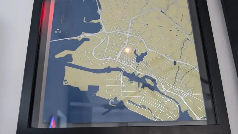
The PCB was designed as a map of the California East Bay area. The roads are laid out as the top-side copper layer, while the land and roads are used for the top solder mask layer, with the flipped land and roads area making up the solder mask on the bottom side. The map data itself was cribbed from Snazzy Maps. Behind the PCB, [Jonathan] mounted a 64 x 32 RGB LED array, which can be seen glowing through from behind the material. The LEDs are controlled by an ESP32, which grabs location data from [Jonathan’s] family member’s mobile devices over MQTT, and uses it to light their positions on the map. Files are on Github for the curious.
If you’ve got a family that is open to location tracking, and the money to pay for a custom PCB, you could probably recreate this project yourself. We’ve seen some other great PCB maps before, too, like this amazing metro tracker. Video after the break.
No comments:
Post a Comment